- 您现在的位置:买卖IC网 > Sheet目录1999 > IDT23S05-1HDCGI (IDT, Integrated Device Technology Inc)IC CLK BUFFER PLL HI DRV 8-SOIC
2
COMMERCIALANDINDUSTRIALTEMPERATURERANGES
IDT23S05
3.3VZERODELAYCLOCKBUFFER,SPREADSPECTRUM
REF
CLK1
2
3
4
8
7
6
5
1
CLK2
GND
CLKOUT
CLK4
VDD
CLK3
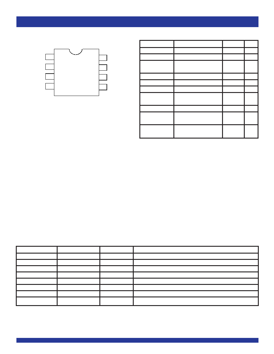
PIN CONFIGURATION
SOIC
TOP VIEW
Symbol
Rating
Max.
Unit
VDD
Supply Voltage Range
–0.5 to +4.6
V
VI(2)
Input Voltage Range (REF)
–0.5 to +5.5
V
VI
InputVoltageRange
–0.5 to
V
(except REF)
VDD+0.5
IIK (VI < 0)
Input Clamp Current
–50
mA
IO (VO = 0 to VDD)
ContinuousOutputCurrent
±50
mA
VDD or GND
ContinuousCurrent
±100
mA
TA = 55°C
Maximum Power Dissipation
0.7
W
(in still air)(3)
TSTG
StorageTemperatureRange
–65 to +150
°C
Operating
CommercialTemperature
0 to +70
°C
Temperature
Range
Operating
IndustrialTemperature
-40 to +85
°C
Temperature
Range
NOTES:
1. Stresses greater than those listed under ABSOLUTE MAXIMUM RATINGS may cause
permanent damage to the device. This is a stress rating only and functional operation
of the device at these or any other conditions above those indicated in the operational
sections of this specification is not implied. Exposure to absolute maximum rating
conditions for extended periods may affect reliability.
2. The input and output negative-voltage ratings may be exceeded if the input and output
clamp-current ratings are observed.
3. The maximum package power dissipation is calculated using a junction temperature
of 150°C and a board trace length of 750 mils.
NOTES:
1. Weak pull down.
2. Weak pull down on all outputs.
PIN DESCRIPTION
ABSOLUTE MAXIMUM RATINGS(1)
APPLICATIONS:
SDRAM
Telecom
Datacom
PC Motherboards/Workstations
Critical Path Delay Designs
Pin Name
Pin Number
Type
Functional Description
REF(1)
1
IN
Input reference clock, 5 Volt tolerant input
CLK2(2)
2
Out
Output clock
CLK1(2)
3
Out
Output clock
GND
4
Ground
CLK3(2)
5
Out
Output clock
VDD
6
PWR
3.3V Supply
CLK4(2)
7
Out
Output clock
CLKOUT(2)
8
Out
Output clock, internal feedback on this pin
发布紧急采购,3分钟左右您将得到回复。
相关PDF资料
IDT23S05E-1HDCGI8
IC CLK BUFFER PLL HI DRV 8-SOIC
IDT23S08-1HPGI8
IC CLK MULT PLL HI DRV 16-TSSOP
IDT23S08T-1DC
IC CLK MULT PLL ZD 2.5V 16-SOIC
IDT23S09T-1DC8
IC CLK BUFFER ZD 2.5V 16-SOIC
IDT5T929-30NLGI
IC CLOCK GENERATOR PREC 28VFQFPN
IDT5T940-10NLGI
IC CLK GENERATOR PREC 28-VFQFPN
IDT5T9820NLI8
IC CLK DRIVER ZD PLL 68-VFQFPN
IDT5T9890NLI8
IC CLK DRIVER 2.5V PLL 68-VFQFPN
相关代理商/技术参数
IDT23S05-1HDCGI8
功能描述:IC CLK BUFFER ZD 3.3V 8-SOIC RoHS:是 类别:集成电路 (IC) >> 时钟/计时 - 时钟发生器,PLL,频率合成器 系列:- 标准包装:1,000 系列:Precision Edge® 类型:时钟/频率合成器 PLL:无 输入:CML,PECL 输出:CML 电路数:1 比率 - 输入:输出:2:1 差分 - 输入:输出:是/是 频率 - 最大:10.7GHz 除法器/乘法器:无/无 电源电压:2.375 V ~ 3.6 V 工作温度:-40°C ~ 85°C 安装类型:表面贴装 封装/外壳:16-VFQFN 裸露焊盘,16-MLF? 供应商设备封装:16-MLF?(3x3) 包装:带卷 (TR) 其它名称:SY58052UMGTRSY58052UMGTR-ND
IDT23S05-1HDCI
功能描述:IC CLK BUFFER PLL HI DRV 8-SOIC RoHS:否 类别:集成电路 (IC) >> 时钟/计时 - 时钟发生器,PLL,频率合成器 系列:- 产品变化通告:Product Discontinuation 04/May/2011 标准包装:96 系列:- 类型:时钟倍频器,零延迟缓冲器 PLL:带旁路 输入:LVTTL 输出:LVTTL 电路数:1 比率 - 输入:输出:1:8 差分 - 输入:输出:无/无 频率 - 最大:133.3MHz 除法器/乘法器:是/无 电源电压:3 V ~ 3.6 V 工作温度:0°C ~ 70°C 安装类型:表面贴装 封装/外壳:16-TSSOP(0.173",4.40mm 宽) 供应商设备封装:16-TSSOP 包装:管件 其它名称:23S08-5HPGG
IDT23S05-1HDCI8
功能描述:IC CLK BUFFER PLL HI DRV 8-SOIC RoHS:否 类别:集成电路 (IC) >> 时钟/计时 - 时钟发生器,PLL,频率合成器 系列:- 产品变化通告:Product Discontinuation 04/May/2011 标准包装:96 系列:- 类型:时钟倍频器,零延迟缓冲器 PLL:带旁路 输入:LVTTL 输出:LVTTL 电路数:1 比率 - 输入:输出:1:8 差分 - 输入:输出:无/无 频率 - 最大:133.3MHz 除法器/乘法器:是/无 电源电压:3 V ~ 3.6 V 工作温度:0°C ~ 70°C 安装类型:表面贴装 封装/外壳:16-TSSOP(0.173",4.40mm 宽) 供应商设备封装:16-TSSOP 包装:管件 其它名称:23S08-5HPGG
IDT23S05E
制造商:IDT 制造商全称:Integrated Device Technology 功能描述:3.3V ZERO DELAY CLOCK BUFFER, SPREAD SPECTRUM COMPATIBLE
IDT23S05E_09
制造商:IDT 制造商全称:Integrated Device Technology 功能描述:3.3V ZERO DELAY CLOCK BUFFER, SPREAD SPECTRUM COMPATIBLE
IDT23S05E-1DC
功能描述:IC CLK BUFFER PLL STD DRV 8-SOIC RoHS:否 类别:集成电路 (IC) >> 时钟/计时 - 时钟发生器,PLL,频率合成器 系列:- 产品变化通告:Product Discontinuation 04/May/2011 标准包装:96 系列:- 类型:时钟倍频器,零延迟缓冲器 PLL:带旁路 输入:LVTTL 输出:LVTTL 电路数:1 比率 - 输入:输出:1:8 差分 - 输入:输出:无/无 频率 - 最大:133.3MHz 除法器/乘法器:是/无 电源电压:3 V ~ 3.6 V 工作温度:0°C ~ 70°C 安装类型:表面贴装 封装/外壳:16-TSSOP(0.173",4.40mm 宽) 供应商设备封装:16-TSSOP 包装:管件 其它名称:23S08-5HPGG
IDT23S05E-1DC8
功能描述:IC CLK BUFFER PLL STD DRV 8-SOIC RoHS:否 类别:集成电路 (IC) >> 时钟/计时 - 时钟发生器,PLL,频率合成器 系列:- 产品变化通告:Product Discontinuation 04/May/2011 标准包装:96 系列:- 类型:时钟倍频器,零延迟缓冲器 PLL:带旁路 输入:LVTTL 输出:LVTTL 电路数:1 比率 - 输入:输出:1:8 差分 - 输入:输出:无/无 频率 - 最大:133.3MHz 除法器/乘法器:是/无 电源电压:3 V ~ 3.6 V 工作温度:0°C ~ 70°C 安装类型:表面贴装 封装/外壳:16-TSSOP(0.173",4.40mm 宽) 供应商设备封装:16-TSSOP 包装:管件 其它名称:23S08-5HPGG
IDT23S05E-1DCG
功能描述:IC CLK BUFFER ZD HI DRIVE 8-SOIC RoHS:是 类别:集成电路 (IC) >> 时钟/计时 - 时钟发生器,PLL,频率合成器 系列:- 标准包装:2,000 系列:- 类型:PLL 频率合成器 PLL:是 输入:晶体 输出:时钟 电路数:1 比率 - 输入:输出:1:1 差分 - 输入:输出:无/无 频率 - 最大:1GHz 除法器/乘法器:是/无 电源电压:4.5 V ~ 5.5 V 工作温度:-20°C ~ 85°C 安装类型:表面贴装 封装/外壳:16-LSSOP(0.175",4.40mm 宽) 供应商设备封装:16-SSOP 包装:带卷 (TR) 其它名称:NJW1504V-TE1-NDNJW1504V-TE1TR